Building a CPU from scratch

I really enjoyed my computer architecture class this semester, however, we never actually built a CPU end-to-end, we only did it conceptually. So during the holidays, I challenged myself to see if I could design my own CPU end-to-end in logism. Lots of fun!
The Basics
MUX (Multiplexers)
Multiplexers, or MUXs, are essential components in digital circuits used to select one input from multiple inputs and forward it to a single output line. Control signals determine which input gets passed to the output. They are commonly used in CPUs for routing data between various components.
Decoders
Decoders convert binary-encoded data into a format suitable for driving specific hardware or components. For example, a decoder takes an instruction opcode and activates the corresponding control signals for execution.
RAM (Random Access Memory)
RAM is a type of volatile memory used to store data and instructions temporarily. In a CPU, RAM interacts closely with registers and the control unit to ensure fast data retrieval and storage during program execution.
Counters
Counters are sequential circuits that increment or decrement values, often used to keep track of program counters or loop iterations in CPUs.
Registers
Registers are small, fast storage locations inside the CPU that hold data, instructions, or intermediate results during computation. They are directly accessible by the processor, making them critical for CPU performance.
Step 1: come up with your own instruction set
An instruction set is the collection of machine-level commands that a CPU understands and executes (aka assembly). Assembly language, a human-readable form of these instructions, is converted into binary by the assembler or compiler for the CPU to process. Instruction sets are specific to the CPU architecture (e.g., x86, ARM).
I recommend starting with this step because the design of your instruction set determines the behaviour of the control unit and other hardware components. Few things to consider:
Instruction Size: Decide how many bits each instruction will have. A typical choice for modern CPUs is 32 bits.
Unique Opcodes: Assign a unique opcode for each instruction type. Opcodes are critical for the control unit to identify which operation to perform.
Register Usage: Specify the number and purpose of registers for each instruction. For instance, some instructions may use two registers, while others might only use one.
Instruction
ADD 0001
SUB 0010
LDUR 0011
STUR 0100
An example of different instructions and their unique opcodes. This is a very very simple instruction set.
Step 2: design the key components of a CPU (the register file, Control Unit, ALU, etc.)
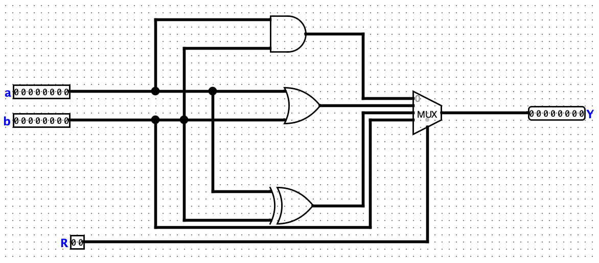
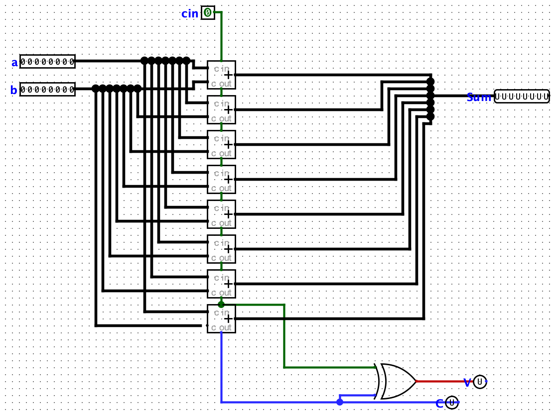
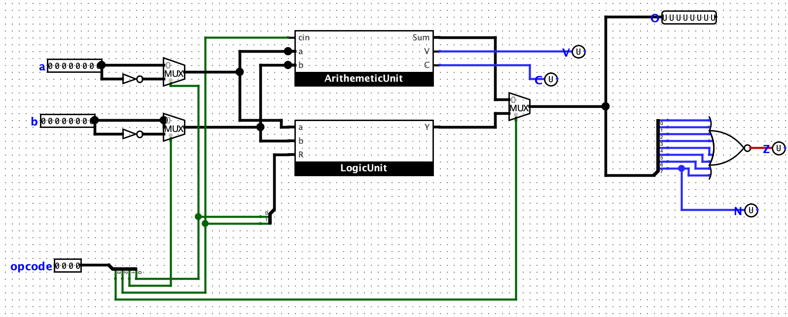
ALU (Arithmetic Logic Unit)
The ALU is the core computational component of the CPU, performing arithmetic operations (e.g., addition, subtraction) and logical operations (e.g., AND, OR, NOR).
Logic Unit: Handles logical operations. It takes two inputs and performs bitwise operations like AND, OR, and NOR. A multiplexer (controlled by the control unit) selects the desired operation's output.
Arithmetic Unit: Handles arithmetic operations. For example, it takes two inputs and adds their bits together. Subtraction is typically implemented by adding the 2's complement of a number.
Putting this together, we take in two inputs and using MUXs and the control unit we decide which data we would like to take, this will depend on the type of instruction being performed, for example, LDUR or STUR will only require in data from one register whereas ADD or SUB will take in two. It’ll also take the opcode which will be fed in as the control line for the logic and arithmetic units as I precisely described above.
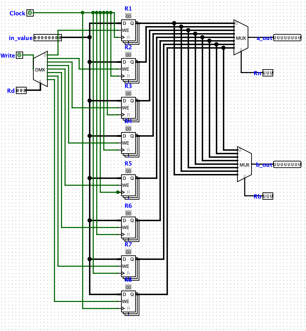
Register files
The register file is a small, fast memory inside the CPU. It stores data that the CPU actively uses during computations. In much more complex CPU designs than what I have done there will be many different types of registers (general and special purpose). For my design, I kept it simple and just had 8 registers and a simple PLC to decide which data to return depending on the input fed in.
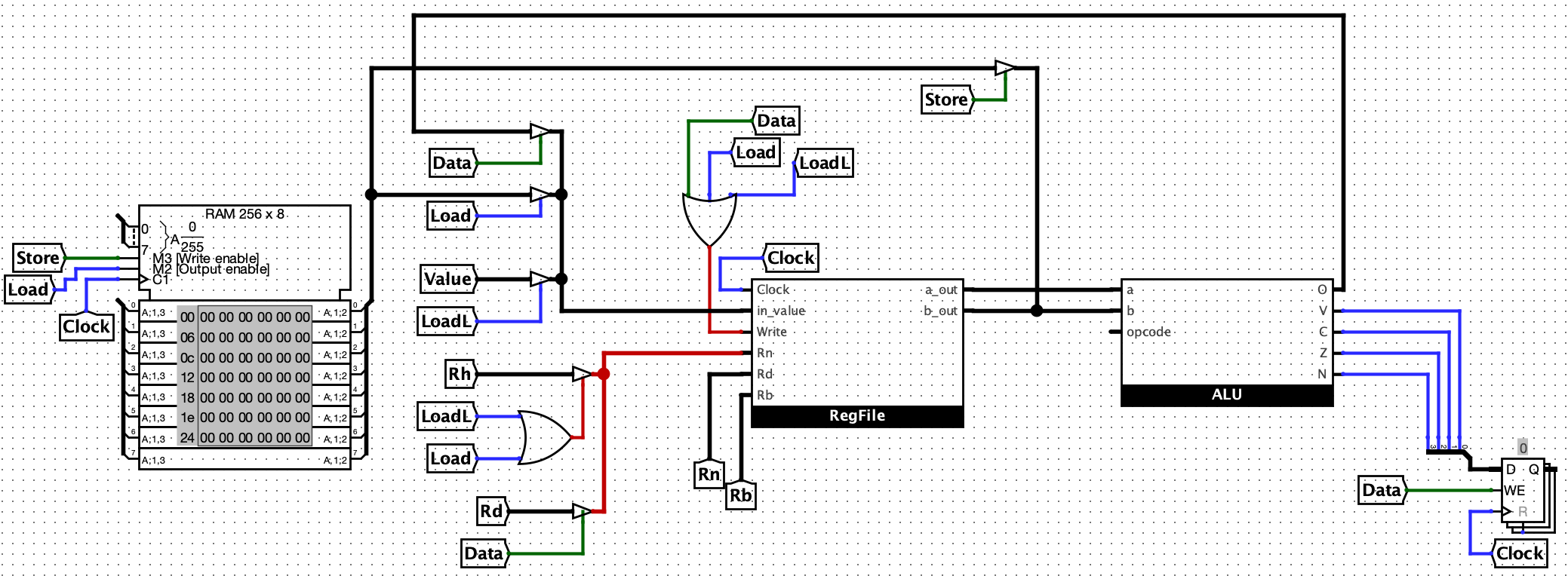
Step 5: build out the single-cycle datapath
In a single-cycle CPU design, each instruction executes in one clock cycle. This means the entire instruction (fetch, decode, execute, memory access, and write-back) must complete within a single clock cycle.
Steps to Build the Single-Cycle Datapath:
Instruction Fetch: Fetch the instruction from memory using the program counter (PC).
Decode: Decode the instruction opcode to generate control signals.
Execute: Use the ALU to perform arithmetic or logical operations.
Memory Access: Read from or write to memory if required (e.g.,
LDUR,STUR).Write-Back: Write the result to a register.
The single-cycle design simplifies the control unit but can lead to inefficiencies if complex instructions require more time to execute.
Key Components:
Control Unit: Decodes opcodes and generates control signals.
Datapath: Includes the ALU, register file, MUXs, and connections for data flow.
By tying everything together, you’ll create a functional single-cycle CPU capable of executing your instruction set.